SN74AHC1G08 SINGLE 2-INPUT POSITIVE-AND GATE
SN74AHC1G08 SINGLE 2-INPUT POSITIVE-AND GATE
SN74AHC1G08 SINGLE 2-INPUT POSITIVE-AND GATE

Create successful ePaper yourself
Turn your PDF publications into a flip-book with our unique Google optimized e-Paper software.
<strong>SN74AHC1G08</strong><br />
<strong>SINGLE</strong> 2-<strong>INPUT</strong> <strong>POSITIVE</strong>-<strong>AND</strong> <strong>GATE</strong><br />
SCLS314A – MARCH 1996 – REVISED MAY 1996<br />
Operating Range: 2-V to 5.5-V V CC<br />
EPIC (Enhanced-Performance Implanted<br />
CMOS) Process<br />
High Latch-Up Immunity Exceeds 250 mA<br />
Per JEDEC Standard JESD-17<br />
Packaged in Plastic Small-Outline<br />
Transistor Package<br />
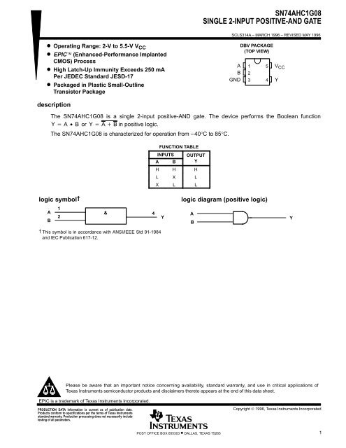
A<br />
B<br />
GND<br />
DBV PACKAGE<br />
(TOP VIEW)<br />
1<br />
2<br />
3<br />
5<br />
4<br />
V CC<br />
Y<br />
description<br />
The <strong>SN74AHC1G08</strong> is a single 2-input positive-<strong>AND</strong> gate. The device performs the Boolean function<br />
Y A • BorYAB in positive logic.<br />
The <strong>SN74AHC1G08</strong> is characterized for operation from –40°C to 85°C.<br />
FUNCTION TABLE<br />
<strong>INPUT</strong>S OUTPUT<br />
A B Y<br />
H H H<br />
L X L<br />
X L L<br />
logic symbol †<br />
logic diagram (positive logic)<br />
A<br />
B<br />
1<br />
2<br />
&<br />
4<br />
Y<br />
A<br />
B<br />
Y<br />
† This symbol is in accordance with ANSI/IEEE Std 91-1984<br />
and IEC Publication 617-12.<br />
Please be aware that an important notice concerning availability, standard warranty, and use in critical applications of<br />
Texas Instruments semiconductor products and disclaimers thereto appears at the end of this data sheet.<br />
EPIC is a trademark of Texas Instruments Incorporated.<br />
PRODUCTION DATA information is current as of publication date.<br />
Products conform to specifications per the terms of Texas Instruments<br />
standard warranty. Production processing does not necessarily include<br />
testing of all parameters.<br />
Copyright © 1996, Texas Instruments Incorporated<br />
POST OFFICE BOX 655303 • DALLAS, TEXAS 75265<br />
1
<strong>SN74AHC1G08</strong><br />
<strong>SINGLE</strong> 2-<strong>INPUT</strong> <strong>POSITIVE</strong>-<strong>AND</strong> <strong>GATE</strong><br />
SCLS314A – MARCH 1996 – REVISED MAY 1996<br />
absolute maximum ratings over operating free-air temperature range (unless otherwise noted) †<br />
Supply voltage range, V CC . . . . . . . . . . . . . . . . . . . . . . . . . . . . . . . . . . . . . . . . . . . . . . . . . . . . . . . . . . –0.5 V to 7 V<br />
Input voltage range, V I (see Note 1) . . . . . . . . . . . . . . . . . . . . . . . . . . . . . . . . . . . . . . . . . . . . . . . . . . . –0.5 V to 7 V<br />
Output voltage range, V O (see Note 1) . . . . . . . . . . . . . . . . . . . . . . . . . . . . . . . . . . . . . . . . –0.5 V to V CC + 0.5 V<br />
Input clamp current, I IK (V I < 0 or V I > V CC ) . . . . . . . . . . . . . . . . . . . . . . . . . . . . . . . . . . . . . . . . . . . . . . . . . – 20 mA<br />
Output clamp current, I OK (V O < 0 or V O > V CC ) . . . . . . . . . . . . . . . . . . . . . . . . . . . . . . . . . . . . . . . . . . . . ± 20 mA<br />
Continuous output current, I O (V O = 0 to V CC ) . . . . . . . . . . . . . . . . . . . . . . . . . . . . . . . . . . . . . . . . . . . . . . ± 25 mA<br />
Continuous current through V CC or GND . . . . . . . . . . . . . . . . . . . . . . . . . . . . . . . . . . . . . . . . . . . . . . . . . . . ± 50 mA<br />
Maximum power dissipation at T A = 55°C (in still air)(see Note 2) . . . . . . . . . . . . . . . . . . . . . . . . . . . . . . 0.2 W<br />
Storage temperature range, T stg . . . . . . . . . . . . . . . . . . . . . . . . . . . . . . . . . . . . . . . . . . . . . . . . . . –65°C to 150°C<br />
† Stresses beyond those listed under “absolute maximum ratings” may cause permanent damage to the device. These are stress ratings only, and<br />
functional operation of the device at these or any other conditions beyond those indicated under “recommended operating conditions” is not<br />
implied. Exposure to absolute-maximum-rated conditions for extended periods may affect device reliability.<br />
NOTES: 1. The input and output voltage ratings may be exceeded if the input and output current ratings are observed.<br />
2. The maximum package power dissipation is calculated using a junction temperature of 150°C and a board trace length of 25<br />
millimeters.<br />
recommended operating conditions (see Note 3)<br />
MIN MAX UNIT<br />
VCC Supply voltage 2 5.5 V<br />
VCC = 2 V 1.5<br />
VIH High-level l input voltage VCC = 3 V 2.1 V<br />
VCC = 5.5 V 3.85<br />
VCC = 2 V 0.5<br />
VIL Low-level l input voltage VCC = 3 V 0.9 V<br />
VCC = 5.5 V 1.65<br />
VI Input voltage 0 5.5 V<br />
VO Output voltage 0 VCC V<br />
VCC = 2 V –50 A<br />
IOH High-level l output current VCC = 3.3 V ± 0.3 V –4<br />
VCC = 5 V ± 0.5 V –8<br />
IOL Low-level l output current VCC = 3.3 V ± 0.3 V 4<br />
VCC = 5 V ± 0.5 V 8<br />
t/v<br />
Input transition rise or fall rate<br />
mA<br />
VCC = 2 V 50 A<br />
VCC = 3.3 V ± 0.3 V 100<br />
VCC = 5 V ± 0.5 V 20<br />
TA Operating free-air temperature –40 85 °C<br />
NOTE 3:<br />
Unused inputs must be held high or low to prevent them from floating.<br />
mA<br />
ns /V<br />
2 POST OFFICE BOX 655303 • DALLAS, TEXAS 75265
<strong>SN74AHC1G08</strong><br />
<strong>SINGLE</strong> 2-<strong>INPUT</strong> <strong>POSITIVE</strong>-<strong>AND</strong> <strong>GATE</strong><br />
SCLS314A – MARCH 1996 – REVISED MAY 1996<br />
electrical characteristics over recommended operating free-air temperature range (unless<br />
otherwise noted)<br />
VOH<br />
VOL<br />
PARAMETER TEST CONDITIONS VCC<br />
TA = 25°C<br />
MIN TYP MAX<br />
2 V 1.9 2 1.9<br />
MIN MAX UNIT<br />
IOH = –50 A<br />
A<br />
3 V 2.9 3 2.9<br />
4.5 V 4.4 4.5 4.4 V<br />
IOH = –4 mA 3 V 2.58 2.48<br />
IOH = –8 mA 4.5 V 3.94 3.8<br />
2 V 0.1 0.1<br />
IOL = 50 A<br />
A<br />
3 V 0.1 0.1<br />
4.5 V 0.1 0.1 V<br />
IOL = 4 mA 3 V 0.36 0.44<br />
IOL = 8 mA 4.5 V 0.36 0.44<br />
II A or B inputs VI = VCC or GND 5.5 V ± 0.1 ± 1 A<br />
ICC VI = VCC or GND, IO = 0 5.5 V 2 20 A<br />
Ci VI = VCC or GND 5 V 4 10 10 pF<br />
switching characteristics over recommended operating free-air temperature range,<br />
V CC = 3.3 V ± 0.3 V (unless otherwise noted) (see Figure 1)<br />
PARAMETER<br />
tPLH<br />
tPHL<br />
tPLH<br />
tPHL<br />
FROM<br />
TO<br />
OUTPUT<br />
TA = 25°C<br />
(<strong>INPUT</strong>)<br />
(OUTPUT) CAPACITANCE MIN TYP MAX<br />
MIN MAX UNIT<br />
AorB Y CL =15pF<br />
6.2 8.8 1 10.5<br />
6.2 8.8 1 10.5<br />
ns<br />
AorB Y CL =50pF<br />
8.7 12.3 1 14<br />
8.7 12.3 1 14<br />
ns<br />
switching characteristics over recommended operating free-air temperature range,<br />
V CC = 5 V ± 0.5 V (unless otherwise noted) (see Figure 1)<br />
PARAMETER<br />
tPLH<br />
tPHL<br />
tPLH<br />
tPHL<br />
FROM<br />
TO<br />
OUTPUT<br />
TA = 25°C<br />
(<strong>INPUT</strong>)<br />
(OUTPUT) CAPACITANCE MIN TYP MAX<br />
MIN MAX UNIT<br />
AorB Y CL =15pF<br />
4.3 5.9 1 7<br />
4.3 5.9 1 7<br />
ns<br />
AorB Y CL =50pF<br />
5.8 7.9 1 9<br />
5.8 7.9 1 9<br />
ns<br />
operating characteristics, V CC = 5 V, T A = 25°C<br />
PARAMETER TEST CONDITIONS TYP UNIT<br />
Cpd Power dissipation capacitance No load, f = 1 MHz 18 pF<br />
POST OFFICE BOX 655303 • DALLAS, TEXAS 75265<br />
3
<strong>SN74AHC1G08</strong><br />
<strong>SINGLE</strong> 2-<strong>INPUT</strong> <strong>POSITIVE</strong>-<strong>AND</strong> <strong>GATE</strong><br />
SCLS314A – MARCH 1996 – REVISED MAY 1996<br />
PARAMETER MEASUREMENT INFORMATION<br />
From Output<br />
Under Test<br />
CL<br />
(see Note A)<br />
Test<br />
Point<br />
Input<br />
(see Note B)<br />
tPLH<br />
50% VCC 50% VCC<br />
tPHL<br />
3 V<br />
0 V<br />
LOAD CIRCUIT<br />
In-Phase<br />
Output<br />
tPHL<br />
50% VCC<br />
VOH<br />
50% VCC<br />
VOL<br />
tPLH<br />
Out-of-Phase<br />
Output<br />
50% VCC<br />
VOH<br />
50% VCC<br />
VOL<br />
VOLTAGE WAVEFORMS<br />
DELAY TIMES<br />
NOTES: A.<br />
B.<br />
CL includes probe and jig capacitance.<br />
All input pulses are supplied by generators having the following characteristics: PRR ≤ 1 MHz, ZO = 50 Ω, tr = 3 ns, tf = 3 ns.<br />
C. The output is measured with one input transition per measurement.<br />
Figure 1. Load Circuit and Voltage Waveforms<br />
4 POST OFFICE BOX 655303 • DALLAS, TEXAS 75265
IMPORTANT NOTICE<br />
Texas Instruments (TI) reserves the right to make changes to its products or to discontinue any semiconductor<br />
product or service without notice, and advises its customers to obtain the latest version of relevant information<br />
to verify, before placing orders, that the information being relied on is current.<br />
TI warrants performance of its semiconductor products and related software to the specifications applicable at<br />
the time of sale in accordance with TI’s standard warranty. Testing and other quality control techniques are<br />
utilized to the extent TI deems necessary to support this warranty. Specific testing of all parameters of each<br />
device is not necessarily performed, except those mandated by government requirements.<br />
Certain applications using semiconductor products may involve potential risks of death, personal injury, or<br />
severe property or environmental damage (“Critical Applications”).<br />
TI SEMICONDUCTOR PRODUCTS ARE NOT DESIGNED, INTENDED, AUTHORIZED, OR WARRANTED<br />
TO BE SUITABLE FOR USE IN LIFE-SUPPORT APPLICATIONS, DEVICES OR SYSTEMS OR OTHER<br />
CRITICAL APPLICATIONS.<br />
Inclusion of TI products in such applications is understood to be fully at the risk of the customer. Use of TI<br />
products in such applications requires the written approval of an appropriate TI officer. Questions concerning<br />
potential risk applications should be directed to TI through a local SC sales office.<br />
In order to minimize risks associated with the customer’s applications, adequate design and operating<br />
safeguards should be provided by the customer to minimize inherent or procedural hazards.<br />
TI assumes no liability for applications assistance, customer product design, software performance, or<br />
infringement of patents or services described herein. Nor does TI warrant or represent that any license, either<br />
express or implied, is granted under any patent right, copyright, mask work right, or other intellectual property<br />
right of TI covering or relating to any combination, machine, or process in which such semiconductor products<br />
or services might be or are used.<br />
Copyright © 1996, Texas Instruments Incorporated