
Back to blog
In-Depth Guide to X-Ray Inspection for PCB Quality Control
Introduction
Printed circuit boards (PCBs) have become exponentially complex over the past decades in terms of component density, layer counts and intricate wiring. This escalating complexity makes effective quality control and defect detection ever more critical. Traditionally, PCB inspection has relied on visual methods like manual microscopy or automated optical inspection (AOI). But these techniques have significant limitations in identifying flaws in multilayer boards or concealed solder joints.
X-ray inspection provides a powerful non-destructive means to peer inside PCBs and accurately pinpoint defects like voids, bridges, open joints etc. This enables catching issues early and preventing field failures down the line. This guide provides a comprehensive overview of PCB x-ray inspection principles, system components, capabilities, benefits over other methods and role in quality assurance processes.
What is X-Ray Inspection for PCBs?

X-ray inspection refers to the use of x-rays to non-destructively examine internal features and subsurface conditions in test objects. It exploits the penetrative nature and differential absorption characteristics of x-rays.
In PCB inspection, x-ray imaging is used to reveal hidden solder joints, component attachments and structural details in multilayer circuit boards which are not accessible by external visual inspection.
X-rays being short wavelength, high frequency electromagnetic waves can penetrate solid objects. When x-rays interact with a PCB test object, variations in material thickness and density across the board result in differential absorption. This creates a projection x-ray image encoding internal structure details which can reveal defects.
How Does PCB X-Ray Inspection Work?
X-ray inspection involves using an x-ray source, test object manipulation system, detector array and processing electronics to produce sample images which are analyzed for defects:
- The x-ray source generates x-rays (either using an x-ray tube or radioactive isotope). This beam is collimated and focused on the PCB sample.
- The PCB is precision positioned and manipulated via a movable stage to enable scanning cross-sections or perspectives.
- Dense solder joints and component materials absorb x-rays more than substrate/resin materials. This creates a pattern of x-ray shadows captured by the detector.
- The detector data is processed to reconstruct a digital 2D or 3D image representation of the PCB’s internal structure.
- Operators examine the x-ray images on inspection monitors to identify any faults like cracks, voids, open joints etc.
- Image processing techniques like subtraction, enhancement and reconstruction aid defect visualization.
Thus, x-ray inspection provides a non-contact means to screen PCBs for hidden flaws frequently missed by external visual checking approaches.
X-Ray Inspection Systems for PCBs
Dedicated x-ray inspection systems are used to perform x-ray imaging analyses on PCBs. These consist of:
X-Ray Source – This generates the x-ray beam. Tube sources using high voltage across a vacuum diode or radioisotopes are common. Control collimators shape the beam.
PCB Manipulation System – High precision robotic stages position and move the PCB sample in the x-ray beam to enable 2D or 3D scanning.
Detectors – Sensor arrays capture the x-rays passing through the board and convert them to electrical signals for image reconstruction.
Image Processing – Hardened processors execute image construction, enhancement and defect recognition algorithms.
Display – High-resolution monitors allow operators to visually inspect the x-ray images for identifying defects.
Shielding – Lead shielding around system protects operators from radiation exposure.
Software – Controls hardware parameters and interlinks system components for automated inspection routines.
These optimized x-ray inspection systems enable repeatable scanning of PCBs from different angles and detection of minute defects.
2D vs 3D X-Ray Inspection
X-ray imaging can produce two-dimensional and three-dimensional representations of a PCB:
2D X-Ray Inspection

- X-ray images are acquired from a single perspective in a single scan.
- Multiple 2D scans from different viewing angles can be combined to enable limited 3D visualization.
- Lower cost method but lacks complete volumetric defect visualization offered by true 3D imaging.
3D X-Ray Inspection

- X-ray CT (computed tomography) imaging constructs a 3D model by assimilating multiple 2D scans around 360°.
- Allows non-destructive visualization of complete internal PCB structure in 3D.
- Enables pinpointing defect locations in 3 dimensions and measuring flaw sizes.
- Provides detailed volumetric data but at higher inspection time and cost.
3D x-ray inspection offers more discerning defect detection for highest reliability PCBs where cost is secondary. For many cases, 2D x-ray inspection suffices in providing PCB cross-section visibility adequate to identify defects and make pass/fail decisions.
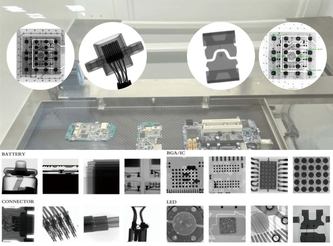
X-Ray Inspection for Components
X-ray imaging is extremely valuable for inspecting PCB components like:
BGA/CSP Packages
- Verifies solder ball attachments below package hidden from view.
- Finds voids, shorts, open joints and insulation problems under component.
- Checks for cracked or damaged silicon die inside package.
- Ensures no PCB pad lifting or trace damage under component.
QFN/DFN Packages
- Inspects J-lead solder joints not visible from top.
- Detects solder voids, insufficient wetting and pad lifting.
- Confirms component alignment with pads.
Connectors
- Checks area array solder joints on connector backs not accessible otherwise.
- Verifies quality of selective, wave or hand soldering.
- Finds bent or improperly seated pins or sockets.
IC Packages
- Allows inspecting hidden solder joints of leaded packages like SOIC, QFP, PLCC etc.
- Screens for shorted pins, tombstoning, skewed parts.
- Confirms adequate slotted pad filling with solder.
- Checks for die damage or cracks.
Passive Components
- Inspects complete circumferential solder joint connections.
- Finds tombstoning, floating or skewed capacitors/resistors.
- Checks for passives placed incorrectly or missing.
Thus, components with concealed attachments are ideal candidates for x-ray inspection to ensure reliability.
X-Ray Inspection for Solder Joints
Since solder alloys contain dense metallic elements like tin, copper or silver, they strongly attenuate x-rays. This allows clear visualization of solder joints inside a PCB:
Discrete Components – Confirm solder joints around leaded components are complete.
SMT Soldering – Verify pad wetting, fillet shapes and sufficient solder.
Plated Through Holes – Check barrel fill quality and shape for through-hole parts.
Vias – Inspect blind and buried vias in multilayers.
BGA/CSP – Detect hidden voids, cracks and shorts under packages.
QFN/DFN – Find amount and shape of paste after reflow under component.
Press-fit Connectors – Ensure proper pin insertion depth and shape.
Hand Soldering – Check joint shape and cold solder joints.
X-ray allows assessing the integrity of solder joints from aspects not possible by visual inspection. This ensures robust joints free of flaws.
Benefits of X-Ray Inspection for PCBs
X-ray inspection delivers multiple advantages over traditional optical inspection methods:
- Non-destructive – No risk of damage to boards or components during inspection.
- See inside PCBs – Ability to peer inside and under components that optical techniques lack.
- Detect hidden flaws – Identify defects like voids and cracks not visible externally.
- Validate solder joint quality – Assess hidden solder joints.
- Map board internals – Constructs 2D and 3D models of PCB internals showing defects in their true locations.
- Dimensional measurements – Can perform measurements of distances, diameters andvolumes.
- Quick inspection – Fast 2D x-ray inspection ideal for production line implementation.
- Analyze fault causes – Helps understand defect occurrences and their root causes.
- High precision – Resolve extremely fine sub-millimeter defects.
- Automation – Software analyzes images automatically and classifies defects using AI.
Thus, x-ray inspection generates invaluable internal defect data no other technique can match. This is crucial for maximizing quality and reliability in PCB manufacturing.
Importance of X-Ray Inspection in PCB Quality Control
Given its ability to detect hidden flaws, x-ray inspection of PCBs provides unique benefits as part of quality assurance processes:
Catch issues early – Identify latent defects from fabrication or assembly before they escape to end products.
Prevent field failures – Avoid failures in customer applications by weeding out defective boards before shipment.
Inspect packaged ICs – Screen for die cracks, wire bonds, lid seal which visual methods cannot.
Audit boards non-destructively – Unlike cross-sectioning or microsectioning which damage boards.
Analyze failure causes – Internal defect visualizations from x-ray aid root cause analysis and corrective actions.
Close the quality loop – Feedback from x-ray failure analysis improves manufacturing and design processes.
Validate process improvements – Quantify reductions in defect rates resulting from process interventions.
Spot trends – Detect evolving defect patterns necessitating manufacturing adjustments.
Supplement AOI – Compensates for limitations of optical inspection in finding subsurface flaws.
Thus, x-ray inspection is an indispensable technique for maximizing quality levels through sensitive defect screening and driving continuous improvements.
Role of X-Ray Inspection in The PCB Quality Workflow
X-ray inspection complements the suite of verification steps implemented during PCB fabrication, assembly and test:
Materials Inspection – Checks consistency of base laminates, prepregs and metal foils.
Bare Board NDT – Tests for shorts, opens, impedance flaws.
Post-Etch Inspection – Verifies conductor structural integrity after etching.
Layer Registration Check – Measures alignment of layers and features across layers.
AOI – Optically inspects populated boards for assembly flaws.
ICT – Tests electrical connectivity of circuits and joints.
Flying Probe – Validates continuity by probing test points.
X-Ray Inspection – Screens for hidden solder defects, cracks etc.
Cross-sectioning – Images conductor interfaces and defects in sliced boards.
SEM – Scans conductor surfaces for lead-free solder joint integrity.
Rework Simulation – Assesses impact of repeated rework on reliability.
The sequence of inspections provides a holistic view of PCB quality from materials to finished boards. X-ray inspection fills the critical gap of identifying subsurface structural and workmanship defects between the external inspection techniques.
Design Considerations to Facilitate X-Ray Inspection
Certain PCB design provisions can enable more effective x-ray inspection:
Test Points – Allows focusing x-rays on specific critical components or nets prone to assembly issues.
Keepouts – Provide adequate clearances around components to allow angled x-ray beam access.
Specialized Features – Include fiducials, markers or symbols to provide image alignment references.
Single-sided Components – Place components only on one side when inspection mainly targets solder joint defects.
Thinner Boards – Reduces x-ray absorption which improves visualization of defects.
Lower Density – Less dense board arrangements simplify analysis versus densely packed configurations.
Dedicated Cutouts – Cutouts under BGAs/CSPs facilitate x-ray imaging of hidden solder joints.
Simulate Defects – Intentionally embed sample defects during prototyping to confirm detection.
Such design-for-x-ray guidelines ensure board structures and layouts are optimized for maximizing visibility of flaws using x-ray inspection equipment.
Limitations and Challenges of X-Ray Inspection
While extremely powerful, certain limitations exist in x-ray inspection approaches:
- Miniaturized electronics with ultra-fine features push against resolution limits of x-ray imaging.
- Low-contrast defects in homogeneous materials are hard to discern in x-ray images.
- Heavy components like large BGAs, connectors or metal shields can block x-rays from revealing underlying features.
- RF, microwave and fiberoptic components need specialized x-ray inspection techniques.
- 2D x-ray lacks full volumetric visualization capability to pinpoint vertical defect positions.
- Operator skill required for analyzing x-ray images and identifying defect signatures.
- Safety procedures mandated for using x-ray equipment add overhead.
- High cost of x-ray inspection systems inhibits widespread deployment across all manufacturing lines.
However, advances in x-ray sources, detectors, image processing and AI assisted defect recognition continue to expand the scope and capability of x-ray inspection for electronics reliability assurance.
Conclusion
The exponential growth in PCB complexity has made non-destructive x-ray imaging an indispensable process for inspecting the interior of multilayer boards. It provides unique defect detection capabilities unmatched by visual inspection methods like AOI, microscopy or image comparators.
For mission-critical aerospace, automotive, medical and defense applications, the benefits of preventing escapes far outweigh the cost of x-ray systems. By thoroughly understanding x-ray inspection principles, artifacts and methodologies, PCB manufacturers can best leverage it to maximize quality levels in their products.
This guide summarizes key considerations in applying x-ray inspection for comprehensively assessing PCB assembly integrity – from subtle solder defects and reliability risks to counterfeit components. Together with optimal usage in the inspection sequence and design-for-x-ray guidelines, PCB manufacturers can realize substantial quality improvements.
Related Articles

5 Ways and Benefits of Determining LED Polarity
Simple schematic diagram of LED polarity judgmentProper placement, labeling, and orientation of components on a Printed Circuit Board (PCB) help reduce common issues such as short-circuiting and other electrical problems. Ensuring correct orientation of components,...
Comprehensive Guide to Electronic HS Codes for PCBA
Export PCBAIn the realm of international trade, HS Codes (Harmonized System codes) are crucial for the classification and categorization of goods. Developed by the World Customs Organization (WCO), these numerical codes provide a standardized method for customs...

Chinese Chips: A Comprehensive Guide for Tech Enthusiasts
Chinese ChipsIn recent years, China's semiconductor industry has experienced a significant transformation, establishing itself as a major player in the global chip market. With advancements in technology and substantial investments in research and development, Chinese...
Take a Quick Quote