Follow Us

How X-Ray PCB Inspection Works
X-ray inspection innovation, also known as automated x-ray inspection, can detect hidden features within a target object. X-ray inspection is a popular method for detecting manufacturing errors in industries ranging from medicine to aerospace. It is especially common in PCB inspection because x-rays are an excellent way to test PCB quality and detect hidden defects without damaging the board.
This guide will explain what x-ray inspection is, how it works, and what benefits it provides, so you can understand how to use PCB x-ray inspection for your company's needs.
Why are X-Ray Machines Popular in Electronics Manufacturing?
Over the last several decades, electronics manufacturing has become increasingly sophisticated, with electronics in the industrial, communication, military, and aerospace industries progressing in ways that make inspection considerably more difficult. Some of the most significant trends affecting inspection include:
Component placement: To save space and maximise functionality, equipment is becoming smaller and more layered. As a result, many solder joints and components are being relocated to inner layers of electronics, either between PCB layers or concealed within the final product itself.- Component size: More PCB components are becoming miniaturised. With the need to produce more dense boards, PCB components are expected to follow suit.
- SMT: Surface mount technology shrinks leads and packages, resulting in higher density PCBs with more components concealed between layers.
Traditional inspection methods have become nearly impossible to use due to the increasing density, decreasing size, and more complex placement of PCBs and their components. Because of the density of modern PCBs, optical, ultrasonic, and thermal imaging methods are relatively ineffective. X-ray inspection, on the other hand, can collect detailed images that other methods cannot. Because X-ray can penetrate PCB layers to inspect inner layers and packaging, it is more useful for inspecting solder joints on complex PCB assemblies. As a result, PCB inspection using x-ray technology is becoming more popular.
How do X-Ray Inspections Work?
To understand x-ray PCB inspection, you must first understand how x-ray inspection works. All x-ray inspection devices share three basic characteristics:
- X-ray tube: This tube is capable of producing x-ray photons.
- Detector: On the other side of the sample, the detector captures and collects x-ray photons, converting them into an image.
- Platform: The sample is moved in different directions by the operation platform, allowing it to be inspected from various angles and magnitudes.
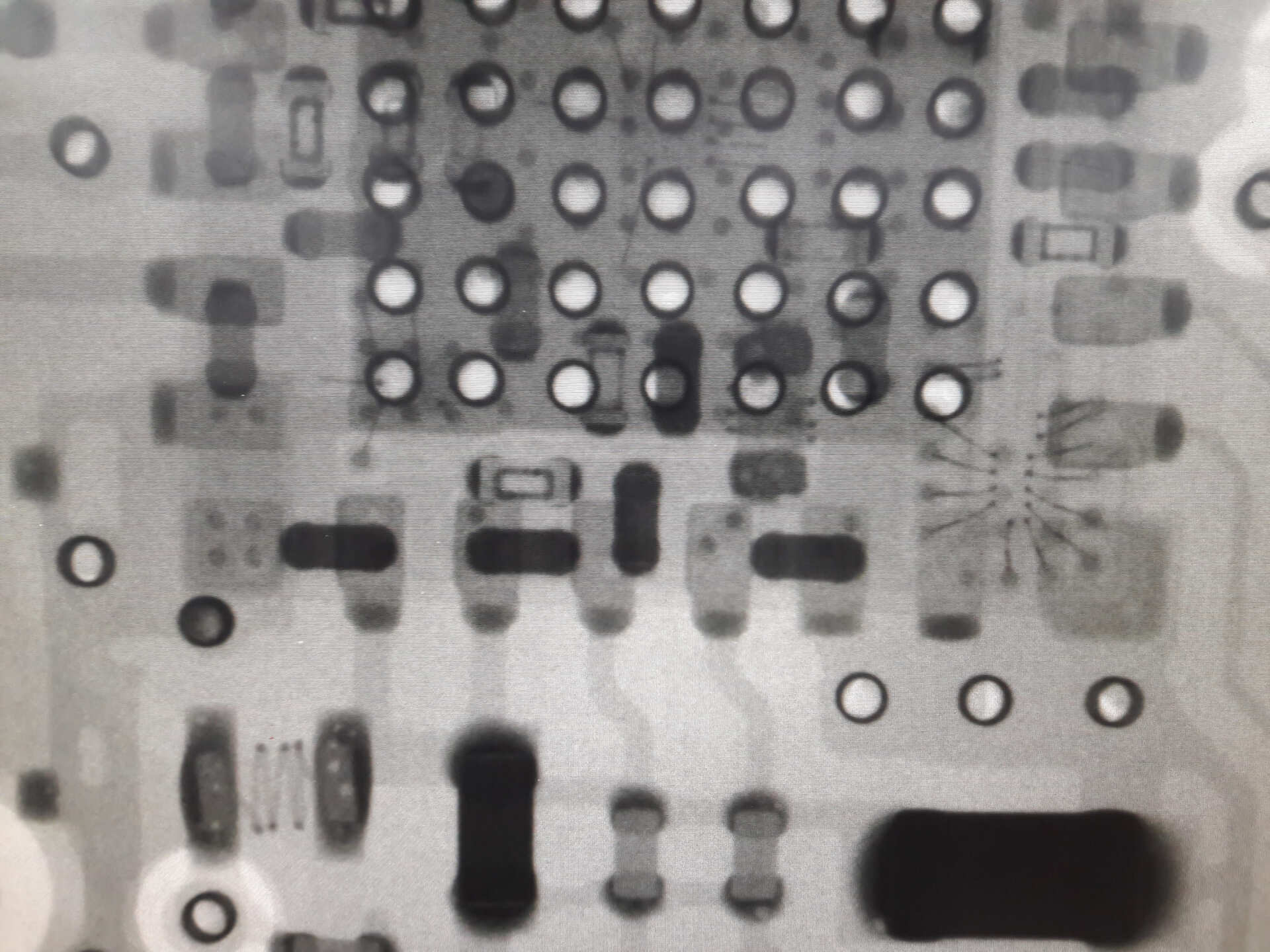
X-ray imaging works by passing x-ray photons through the material and collecting them on the other side. The physical properties of materials, such as atomic weight, density, and thickness, affect how x-ray photons pass through them. Heavy elements, in general, accumulate more x-ray photons, making them easier to image, whereas lighter elements are more transparent. Because various materials behave differently, varying amounts of photons are gathered on the other side of the object, producing an image. Components on a PCB are typically made up of heavier elements, making them visible on an x-ray image.
Benefits of X-Ray Inspections
Metal is dark in x-ray images of PCBs, whereas glass, plastic, and ceramics are translucent. This makes metallic components visible. When combined with magnification, this enables inspectors to see different metallic parts on a board during PCB inspection with x-ray equipment. Inspectors will be able to see multiple qualities of a printed circuit and recognise a variety of potential problems using the x-ray, including:
Solder bridges: On circuit boards, solder bridges are a common issue. This happens when solder joints are too close together or when a connection is formed where there should be none. These solder problems are usually hidden by other components, making optical inspections difficult to detect, but x-rays easily identify them.- Solder voids: Solder voids are formed when gas or flux is trapped during soldering, which is frequently caused by water contamination of the solder paste. These voids reduce heat conductivity at the solder joint, which can lead to physical defects and decreased reliability. Because X-ray is one of the only methods for detecting solder voids, it must be used regularly to ensure product and process quality.
- Pin-hole fills: Insufficient pin-hole fill for through-hole connectors is a common problem in circuit boards. X-ray machines can detect these errors and even quantify the amount of fill that is missing by using coordinate measurements.
A ball grid array (BGA) inspection is one example of how an x-ray is used. A BGA is a surface mount device that connects via an array of metal spheres made of solder. This device is popular because it allows for high-density connections without affecting PCB layouts. The problem with BGAs is that the components are connected to the underside of the chip. This feature, along with the density of the solder balls, makes soldering and desoldering difficult and increases the likelihood of solder bridges forming. The location also makes inspecting BGA chip solder joints, especially challenging. By having to look through the device to see the solder joints underneath and easily identify bridges, an X-ray simplifies the inspection process.
X-ray machines with magnification and the ability to change the viewing angle can be used to detect these and other issues. Even better, because, unlike medical imaging, technicians do not need to worry about radiation dose during the procedure and can use the devices for as long as they need.
Why Choose M-Tek Assembly Ltd
Here at M-Tek Assembly Ltd, we are proud to announce that we are now certified carbon neutral. For every circuit board we build, we plant a tree in Uganda. We are working hard to be environmentally responsible and help you reduce your carbon footprint by working with us. With M-Tek, we believe the customer always comes first! That is why we pride ourselves on our commitment to existing and new customers alike with our rapid responses and continue to expand our excellent quality services into new sectors and industries.
To learn more about what we do or if you need a PCB x-ray inspection, get in touch with a member of the M-Tek team today by calling 01189 455 377 or following us on
Twitter.
Recent Posts


Share This Post
Leave A Comment
Contact Us
Contact Us - Blog

M-Tek Assembly. A Specialist Full Turnkey Electronic Manufacturing Partner. Full Procurement, Assembly, X-RAY, Programming & Test Services
