
Automated PCB X-ray inspection is an important quality control technology using either 2D or 3D X-ray imaging to detect defects in products during the production process. AXI complements automated optical inspection (AOI) by detecting defects that are invisible to optical cameras such as voids in ball grid arrays (BGAs), widely used in surface mount packaging. Different types of X-ray detector can be used for the automated inspection of PCBs, but which type is the best suited to the task?
NIC PCB X-ray
In the early days of PCB inspection, image intensifier tubes coupled to CCD cameras were widely used. These were smaller six inch diameter versions of the image intensifiers used for surgical C-arm and interventional radiography in the last century, which were typically nine or twelve inches. Image intensifiers had the advantage of good spatial resolution combined with video frame rates, low electronic noise from the CCD sensor and very high gain, resulting in high sensitivity even at the low dose rates found in high frame rate X-ray imaging. The same qualities made CCDs a good choice for surgery.
Amorphous silicon flat panel detectors were introduced in medical imaging from about 2000. They were mainly used in high dose applications such as mammography and general radiography, but did not displace the image intensifier in surgical C-arms where image intensifiers remained the dominant technology due to their superior spatial resolution and image quality at video frame rates in low dose fluoroscopy. Small amorphous silicon flat panel detectors made by Varian with 127 micron pixel pitch were used in some AXI products but these suffered from modest frame rates, large pixel pitch and relatively high electronic noise compared to CCDs.

Dexela CMOS X-ray Detectors. (Image from Comparison of CMOS and a-Si flat panel imagers for X-ray imaging G. Zentai Published 17 May 2011 Physics. 2011 IEEE International Conference on Imaging Systems and Techniques)
In 2009, Dexela introduced high speed, large area CMOS X-ray detectors with 75 micron pixel pitch: 1512, 2315 and 2923. These were widely adopted for AXI by companies in UK, Europe, Japan, Korea and China and became the market leader for AXI and offline PCB inspection. The Dexela CMOS detectors were comprised of arrays of one or more large area CMOS images sensors bonded to fibre optic plates (FOPs) and coupled to thallium doped caesium iodide (CsI) scintillators.

SEM image of Caesium Iodide (CsI). PIcture courtesy of Scintacor
The key to the success of CMOS flat panel detectors was the combination of high frame rates, low electronic noise in the sensor, high spatial resolution, virtually no image lag in the sensor, good image quality at low dose and good reliability. For the same reasons, CMOS detectors from Dexela and subsequently Dalsa came to dominate the surgical C-arm market displacing amorphous silicon from all but the cheapest C-arms, which benefit from the very low production cost of amorphous silicon flat panels. In 2020, Spectrum Logic launched a family of next generation CMOS detectors specifically designed for AXI – 0606, 1206, 1412 and 2824. These used a proprietary high speed column parallel ADCs design that achieved a unique combination of low electronic noise, low image lag, high frame rate and high spatial resolution with 50 micron or 100 micron pixel pitch.

Spectrum Logic 1206HR X-ray Detector
A variant on amorphous silicon was introduced in 2020-2023 called IGZO. IGZO has similar properties to amorphous silicon and has been adopted in some surgical C-arms. It has superior performance to amorphous silicon but is inferior to CMOS. However, despite early optimism, it has not been widely adopted in AXI because it is easily damaged by X-ray radiation. For this reason and the lower imaging performance than CMOS, IGZO is not normally offered for AXI.
Both amorphous silicon and CMOS flat panel detectors typically use CsI scintillators to convert X-ray photons into visible light that can be detected by image sensors.

How CsI scintillators convert X-ray Photons into visible light to be detected by image sensors
This indirect detection technology is mature and effective, but direct detection is also possible using room temperature semiconductor detectors such as amorphous selenium, cadmium telluride (CdTe) or cadmium zinc telluride (CZT). Amorphous selenium is popular in mammography because it is reasonably efficient for low energy X-ray and is available in large area detectors. However, it has not been adopted in AXI because it is inefficient at the higher energies used for AXI (70 to 160 kV), has substantial image lag and is unstable in high or low temperature environments. Other direct detection products have been produced using CdTe or CZT. These materials have a high atomic number making them efficient at the X-ray energies used in AXI. The most successful product of this type in industrial applications was introduced by Ajat and then acquired by XCounter, which changed its name to Direct Conversion and was acquired by Varex Imaging in 2019. It is popular in dental panoramic and food inspection markets where it is used as a linear scanning detector replacing CCDs operated in TDI mode. However, so far it has not been possible to product a large area CdTe or CZT detector with the required spatial resolution for use in AXI at a reasonable cost and this technology has, as a result, been unable to penetrate the AXI market despite its high efficiency and high frame rate.

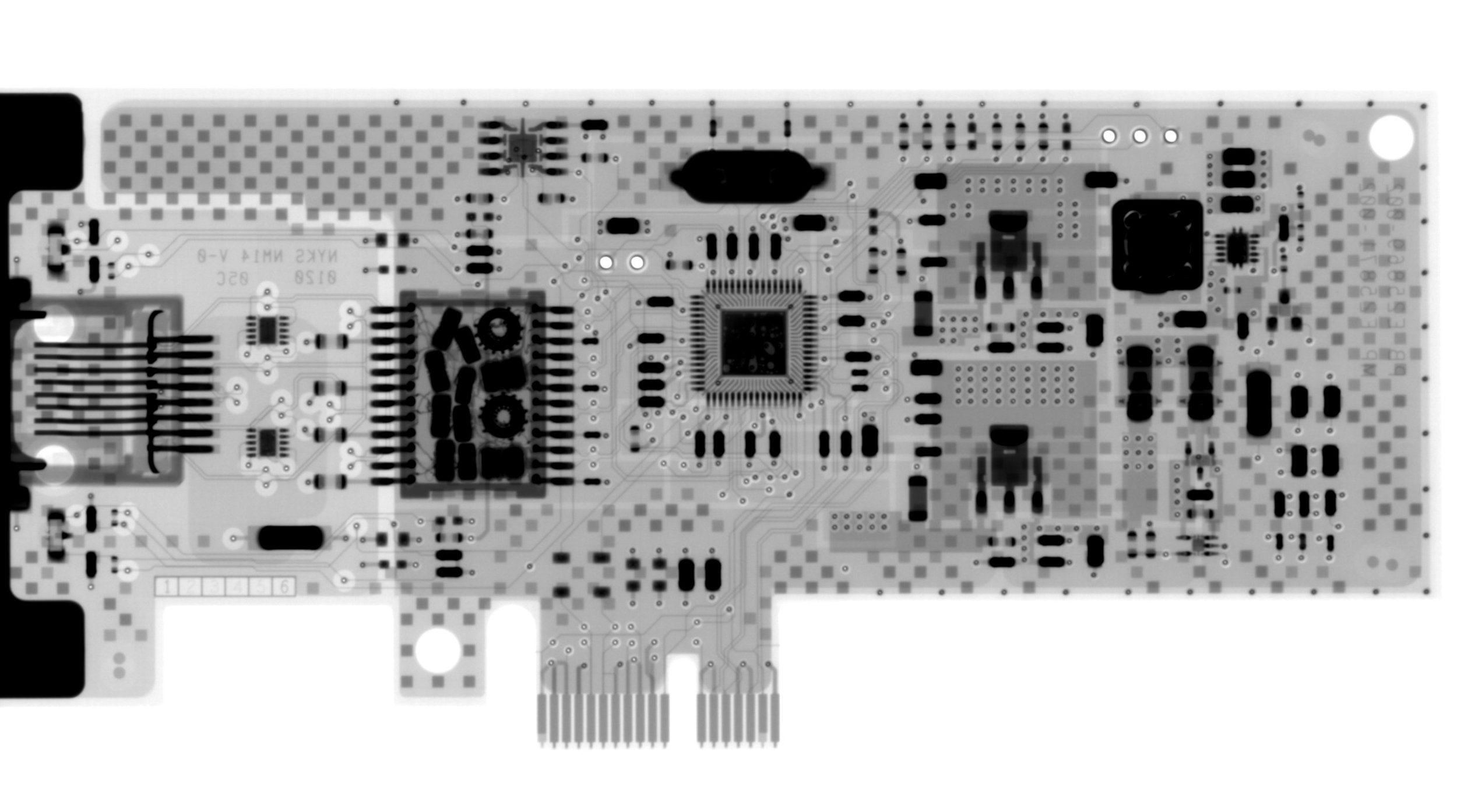
PCB X-ray Image taken using Spectrum Logic 1412HR
In summary, here are the advantages of using large area CMOS detectors with FOPs and CsI scintillators for PCB inspection:
· High efficiency: CsI scintillators can absorb a large percentage of the x-rays that are incident on them, which means that they can produce high-quality images with good contrast at high frame rates.
· High resolution: CMOS detectors can resolve small features on a PCB, which makes them well-suited for detecting defects such as voids in balls, missing components, and cracks.
· Reliability and radiation tolerance: CMOS detectors with FOPs can tolerate large radiation doses without failing and are not highly sensitive to environmental fluctuations such as high or low temperature.
· High frame rate: the high frame rates offered by modern large area CMOS detectors permit high testing throughput.
· Large active area: modern CMOS detectors are available from 6 x 6 cm to 31 by 31 cm.
· Cost-effective: CMOS detectors are relatively inexpensive and have a low total cost of ownership.
If you are looking for an x-ray detector for PCB inspection, a modern CMOS detector with an FOP is the best option. They offer the best combination of sensitivity, resolution, speed and cost, making them ideal for this application.